Surface Atomic Structure
From Seeing to Moving Atoms
The first microscope that can “see” atoms was the field ion microscope invented by Muller and Bahadur in 1955. The transmission electron microscope reached atomic resolution for the first time in 1970. Although the invention of scanning tunneling microscope (STM) by Binnig and Rohrer was much later than other two technologies, its important role can never be underestimated. Scanning tunneling microscope is an imaging technology to characterize the surface structure of matters with an atomic resolution. Besides “seeing” atoms, it can also be used to move atoms on the surface. In 1990, scientist from IBM used STM to place 35 Xenon atoms into “IBM”, which was regarded as an important milestone in the history of science.
The atomic force microscope was developed based on the principle of STM and has become one of the most important research instruments for scientists to study the surface microstructures. AFM was invented by IBM’s scientists in 1986. It is noteworthy that Binnig was also one of those scientists. Both AFM and STM are scanning probe microscopes. STM relies on the quantum tunneling effect between the probe and the sample to detect the surface structure. Even though STM can image a single atom, it cannot provide position and bonding information for all atoms in an organic molecule (the reason can be explained by quantum mechanics). AFM utilized the interaction between the probe and the sample to observe the surface. In theory, were the probe sharp enough we would be able to acquire all position and bonding information of atoms in a molecule simultaneously. This has been a dream for chemists and it was finally realized by scientists from IBM, who successfully imaged all atoms and bonds in a pentacene molecule by fixing a carbon monoxide molecule at the tip of an AFM probe. This technology was developed rapidly. In 2013, scientists from Berkeley captured how a single molecule changed its configuration before and after a chemical reaction with an AFM. Chinese scientists from National Center for Nano Science and Technology also used an AFM to observe hydrogen bonds for the first time. It is believed that more and more secrets in the molecular world will be revealed by STM and AFM.
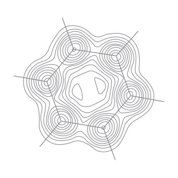
Top diagram: a quantum coral made by a scanning tunneling microscope. Ref.: Crommie, M. F. et al. Science 262, 218 (1993).
Scanning tunneling microscope. Binnig and Rohrer invented the scanning tunneling microscope in 1981, which has been an important experiment instrument to study the surface property of matters at an atomic scale. They also won the Nobel Prize in physics in 1986 due to this invention. In 1983, Binnig and Rohrer investigated using STM one of the great challenges to surface scientists, the 7×7 reconstruction on the Si (111) surface. The image (illustrated in the left figure) demonstrated the surface unit cell with 14 adatoms, providing critical evidence to solve the 7×7 reconstruction. [Figure reference: Binnig, G. et al. Phys. Rev. Lett. 50, 120 (1983)]
The surface reconstruction of silicon. From the discovery of the 7×7 reconstruction on the Si (111) surface in 1959, it took more than 25 years until Takayanagi proposed the widely recognized dimer-adatom-stacking fault model (DAS). Before DAS model, there have been more than twenty incorrect models. The STM image by Binnig and Rohrer provided important evidence for DAS. The above image is an illustration of the 7×7 reconstruction in Takayanagi’s paper, where white and green colors represent adatom and dimers, respectively. Cutting a crystal will make many surface atoms be in a higher energy state because they have lost neighboring atoms. In order to lower the surface energy, reconstruction will occur for those atoms on the surface and result in a surface structure different from the crystal structure. [Figure reference: Takayanagi, K. Surf. Sci. 164, 367 (1985)]
The smallest movie in the world. STM can also be used to move atoms to obtain incredible small structures. In 1990, scientists from IBM placed 35 Xenon atoms on the surface of nickel by STM and arranged them into the letters of “IBM”. In 2014, it was still the scientists from IBM that came up with a fantastic idea. They created the smallest stop motion animation film, a Boy and His Atoms, by moving thousands of CO molecules on the metal surface by STM tips. In the above figure, each blue dot represents a CO molecule, and the grey grid indicates the possible adsorption position on the metal surface for CO molecules. Each figure is drawn according to a movie screenshot. Heinrich, the producer of the movie, suggested that by making this movie it would be delighted to have 1,000 kids join the science camp instead of entering law school. In addition, Heinrich’s group in 2012 found that 12 atoms were the upper limit for a magnetic storage unit through STM. Nevertheless, each magnetic storage unit contains more than 1000 atoms in the present hard drives, indicating that there is still plenty of room to improve the storage density. [Figure reference: A Boy and His Atom (2014)]
Other Topics


